Updated March 2019: This design was originally published as a 500mW output transmitter, but the author has now implemented and tested a 1W output version.
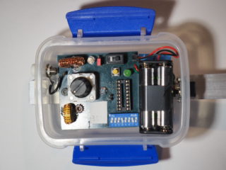
500mw version in a 200ml FOOD BOX with 4xAAA BATTERY PACK
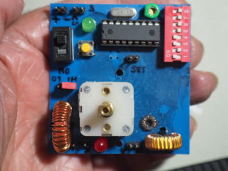
PROTOTYPE BOARD
This 80m ARDF transmitter was designed to be multi purpose, suitable for Classic (1W minimum) , Sprint (300mW-1W) and FoxOring formats.
Compact and lightweight and easy to deploy.
Low component count.
Multipurpose socket for charging/syncro/tune-up.
Internal ATU for matching to a short wire antenna.
A minimum of 1 watt output is required for Official Classic competition, but the lower power should be adequate for local events.
CIRCUIT DESCRIPTION
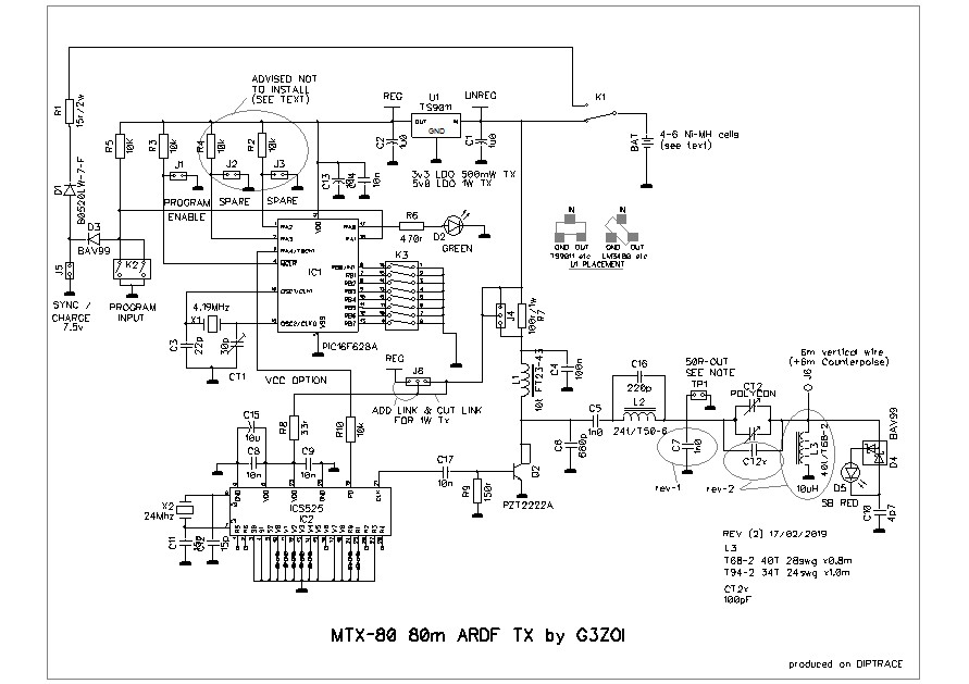 The 80m source signal is derived from a digital clock multiplier, the ICS525-01 using a 24MHz xtal.
( Note: the ICS525-02/3 has different output dividers, so is not suitable )
The ICS frequency configuration was derived from a design by SM0KON. This allows for a selection of a frequencies between 3510 Khz and 3610Khz at 10kHz steps by setting the high/low status of just 7 configuration pins on the IC. The other 12 configuration pins are fixed in the PCB layout.
The 7 pins can be set high or low by cutting or grounding pads on the PCB.
WARNING (500mW version only) . The ICS chip supply voltage is unregulated and direct from the battery supply. The maximum voltage should not exceed that supplied by 4 ni-mh cells ie. 5v nominal, 5.8v maximum at full charge . Please read the full documentation for more information .
POWER OUTPUT CIRCUIT
The original design used a pair of 2N7002s, giving 1 watt output, but these proved to be quite fragile so were replaced with a single IRLML0100.
However it was found that both MOSFET devices drew high current when the ATU was miss-tuned. No simple solution was found to solve this, so the PA device was changed to a PTZ2222A with a lower output , but more stable output of 500mW.
In order to achieve 1W output it is necessary to increase the supply voltage to 7.2v using 6 ni-mh cells. In this case the pcb has to be modified, using a 5v LDO regulator so that a regulated 5v volts is supplied to both the PIC and the ICS driver. (refer to documentation)
A pi network provides a 50 ohm match at the TP1 test point. Then a L network to match a long wire (see text below). C16 and L2 provide a trap to reduce 2nd harmonic radiation.
The output matching was optimize by trial and error. The filtering is minimal, but in the context of ARDF deployment, is considered acceptable. If this design is used or modified for any other purpose the user should be satisfied the filtering is sufficient to suppress harmonic or spurious emissions.
The ATU section of CT2 and L3 is the L-network designed to match a 6m long wire with a 6m counterpoise. A set of precut antenna wire is required for the ARDF event, so the user should decide the preferred length of the wire antenna and modify the turns on the toroid (L3) to suit.
8m wire length is a popular traditional choice, but the author finds 5 or 6m lengths work well enough and are easier to deploy.
Of course, other (usually shorter lengths) can still be connected and tuned but the ATU may not be optimal.
CHARGING / SYNCING SOCKET
The charging socket has three functions.
1. Charge the battery.
2. Synchronize the Txs.
3. Key the transmitter (when idle).
You can use the same cable for both charging and Synchronizing.
Obtain a 6 way, daisy chain, 2.1mm power cable. These are readily and cheaply available on eBay (for guitar amplifiers!). Synchronizing requires an external shorting switch connected to an inline power plug.
WARNING. After synchronizing, do not close the shorting switch until the cable is removed. If the transmitters are running in delay mode, this will key-up all the transmitters!
DOWNLOADS
MTX80C1.zip 02-04-2018
MTX80C2.zip 25-04-2018 Output Network & ATU revised
MTX80C3.zip 07-05-2018 BOM corrections & additional photos.
MTX80C4.zip 23-04-2019 Updated for 1 watt output version.
Detailed Documentation
- Schematic
- Material list
- PCB track image
- PCB parts layout TOP
- PCB parts layout BOTTOM
- SOFTWARE SOURCE CODE
- SOFTWARE HEX CODE FOR 16F628A
- Photos showing track modifications.
If and when PCBs are available for purchase, they will be listed on EBAY.
click here to check
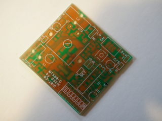
TOP SIDE
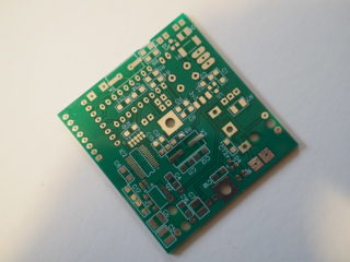
BOTTOM SIDE
NEW – 500mW 80m TX
UPDATE AVAILABLE
Hello David,
Thank you for your posts.
In order to build small training TX I work with PLL sintez (button operated).
What the difference between ICS525-01 and 02 versus? In sofware calculator they are the same.
Have you tried using ICS525-02 for 3.51-3.60 MHz?
The output dividers are different. The ICS525-01 in the TX uses a divider value of 10, which is not available in the ICS525-02.